Trace & via current carrying capacity on PCBs from JLCPCB
If you ever designed your own printed circuit board, you might have wondered “how thick does this trace needs to be?” or “how big this via needs to be?”. As always, you can try to Google it – however, you will find a lot of conflicting information, and that is why I ordered a simple PCB from JLCPCB and measured some of these characteristics.
Note: I am by no way paid, endorsed or anything like that by JLCPCB. I am simply giving you the name of the manufacturer whose product I used for my experiments.
Chapter 1: trace thickness
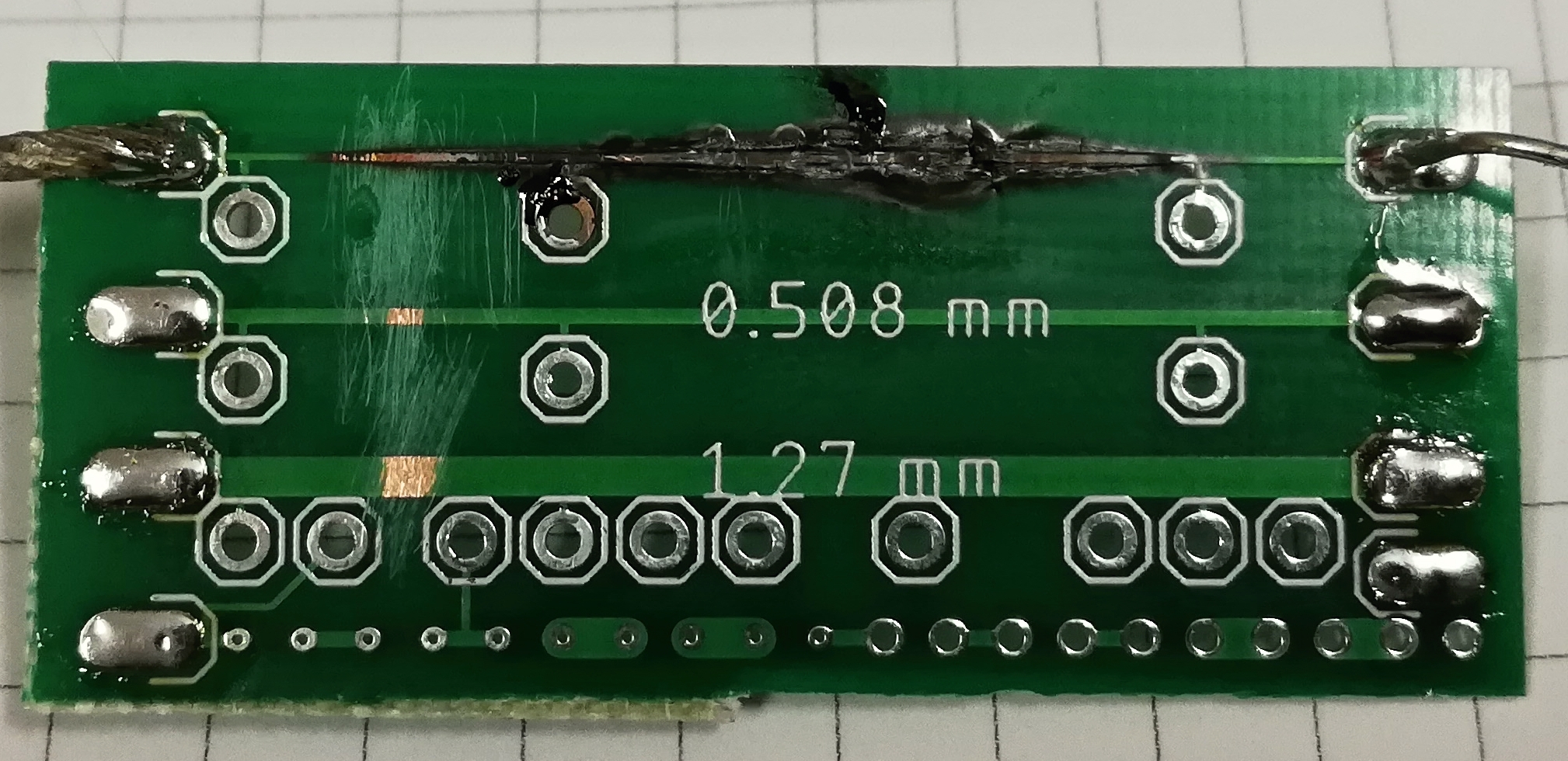
First thing I wanted to evaluate was the actual thickness of a trace. The manufacturer claims it is 35 μm, or 1 oz/ft, so it is too thin to be measured by a mechanical meter (at least by any meter I have at home). So my test setup was simple – I just ran different currents thru different traces and measured the voltage on a given length with a precise voltmeter (using Kelvin’s connection, of course). Then, knowing the resistivity of copper, I calculated the cross section and from that the thickness.
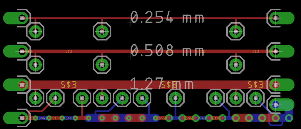
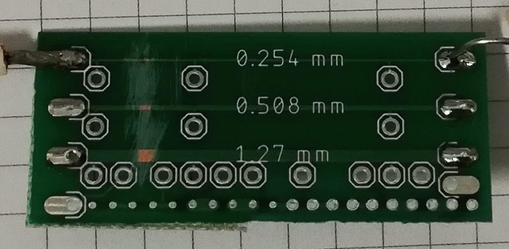
I used current from 150 mA to 4 A on the thicker traces and trace widths of 0.254, 0.508 and 1.27 mm.
Results: all of my measurements (and there were a lot of them) returned values between 28.25 and 29.03 μm, which is only about 81 % of what the manufacturer promises. You can download all the raw data from here.
Possible mistakes: I used really precise instruments and really precise distance between probes. I made regular breaks between measurements to reduce the error due to heating of the trace. So there are only two things which might be wrong – either the traces are narrower then they should be or JLCPCB uses some sort of copper alloy with higher resistivity than normal copper.
Chapter 2: trace temperature rise
Of course it is hard to define maximal trace current – I bet you can run 4 amps thru 0.254 mm trace, at least for a very short time (see the last picture, I actually tried that). So I measured the approximate current at which the trace will heat up 10 °C from ambient. This should give me a rough estimation of safe current, even though another thing to consider is the voltage drop across such a trace.
Results: with the ambient temperature of 18 °C, the 0.254 mm could handle 800 mA just fine; the 0.504 could handle 1.4 amps and the thickest, 1.27 mm trace was capable of handling 2.5 amps. These values are high, but as I mentioned before, the voltage drop at such a current is another thing to consider. But anyways, these currents roughly equal to the output of this calculator.
Chapter 3: via resistance
Another thing I was interested in was how much current can a via actually carry? And how does it depend on the via drill diameter?
For that, I used the bottom part of my board and here are the results: 0.35 drill via with 0.75 mm outer ring has a resistance of about 0.8 mΩ; 0.7 drill via with 1.1 mm outer ring has a resistance of about 0.45 mΩ . All of this was done on a 0.8 mm thick PCB.
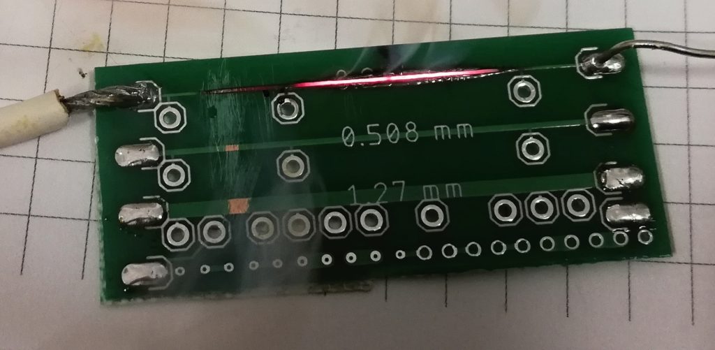
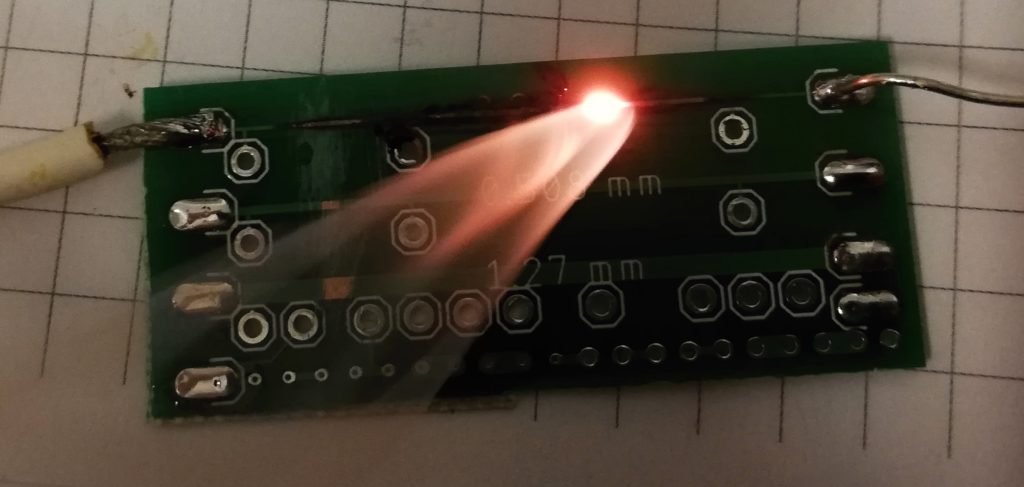
Chapter 4: destructive testing
Just for fun I tried how much current it takes to really destroy the thin 0.254 mm trace . You can see the pictures below, but basically at 3 amps, the temperature jumped to roughly 170 degrees celsius, some sort of vapor started leaking from the board and it started smelling really really bad. But that was all, no fire. So I cranked up my power supply to 4 amps and the trace got immediately red hot, a flame showed up and in a few seconds it turned sort of a small fireball. But even after half a minute, it still did not break the electrical connection and the small fireball was there. I had to turn of the power supply however, because all the dense cancerous smoke started filling the room…
Chapter 5: conclusion
You can safely use the 0.254 mm thick trace even to power microprocessors, if you don’t have enough space on a PCB. In other words, it can be used up to 800 mA. The 0.508 mm trace can be used up to 1.4 amps and the 1.27 mm trace can carry up to 2.5 amps without significant heating. Vias have very low resistance and even a 0.35 mm drill via can safely carry 2 amps of current. Furthermore, their resistance can be reduced by filling them with solder.
good, I was trying to calculate the track width to 5A using the calculator you left on the link to use.
but I have some doubts.
I changed the ampere value to 5 amperes, and I changed the Thickness to 1.
Two frames appeared with the Results for Internal Layers
and other Results for Internal Layers
which one is it?
you only need to change the amperage and thickness values ?
Hi,
well, I cannot replicate that behaviour – when I input your values, I don’t get any extra ‘frames’. So for me, the result is cca 7 mm internal/3 mm external. Do note though that that’s for 10 degC rise, you can usually push it a little bit more (30 degC is still considered ok).