
Quick Charge 3.0 circuit
Generally speaking, the USB interface is pretty complicated. This is also true if you want to charge or just deliver some power over USB – normally, USB-compatible devices will only dare to draw up to 500 mA, which isn’t much and it means a full charge of a battery would take hours. If you want to charge at, let’s say, 2 amps, you need to let the device know that it can actually draw that much current from the USB socket – and unfortunately, there are many specifications and protocols used to do that, from USB DCP (Dedicated Charging Port) which shortens the D+ and D- lines, to Apple’s own protocol, which applies particular voltages to the data lines and so on.
Additionally, some protocols even raise the VBUS voltage. Normally, the VBUS is +5 V, which limits the delivered power to 10 W (at 2 A, which is the limit of most connectors and cables), but some recent protocols like Quick Charge (Qualcomm), Fast Charge (Huawei) and USB Power Delivery started increasing the VBUS voltage up to 20 V, in order to deliver more power over the same wire thickness. More power of course means quicker charging and that is what everybody wants.
I do own a couple of devices which support one of the abovementioned protocols, and so when I was thinking about designing my own powerbank, I wanted it to have support for at least Quick Charge. So I started looking into how to design a QC-compatible USB port, but there weren’t really that many circuits on the internet. But in the end, I’ve succeded in creating a very well working circuit and here I’d like to share it.
Attempt #1 – QC 2.0
My first attempt was based on an IC I found over on LCSC.com – the SE100 in SO-8 package:
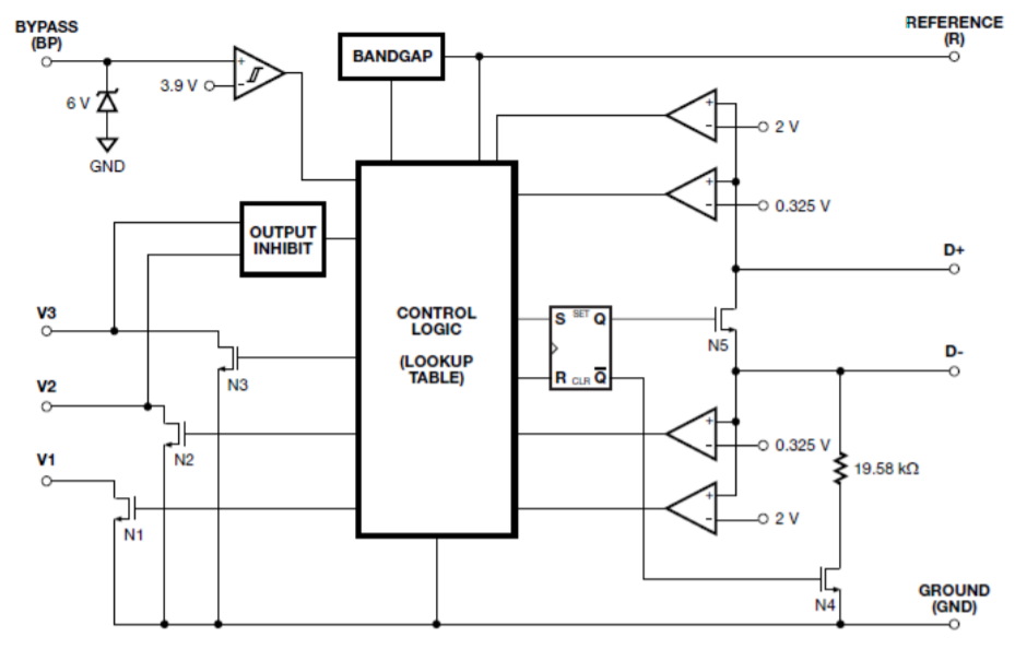
It’s an IC supporting QC 2.0 and a lot of other protocols. It’s working principle is simple – you have an external switching converter (either buck or boost, does not really matter) and such a converter usually has a resistive divider to monitor the output voltage. The middle of this divider is connected to a feedback pin and the converter adjusts it’s output in such a way that the feedback pin voltage is some predefined value – usually 0.6 or 1.2 V.
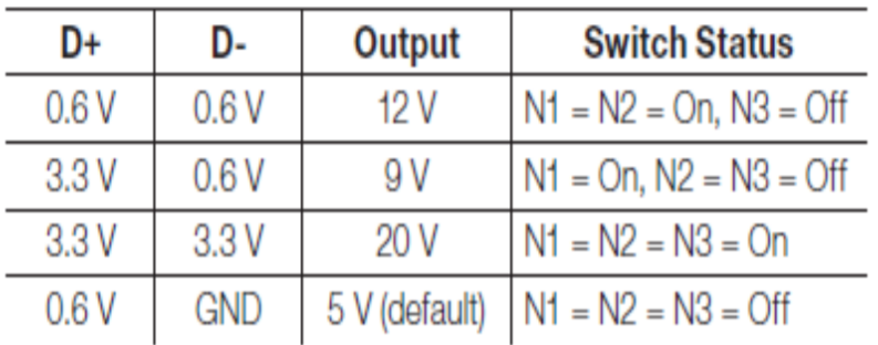
The SE100 has three open drain pins (called V1 to V3) – they are basically the collectors (or drains) of three transistors, which are switched on in a particular manner, based on the desired output voltage (detected by the QC interface). You can find these ON-OFF patterns in this table taken from the datasheet:
So what you do is you add three resistors, connect them to these pins on one side and to the center of the resistive divider (ie the FB pin) on the other side. If the SE100 detects a QC-compatible device, it enables some of the transistors, which basically puts the corresponding resistors in parallel with the lower feedback resistor. This lowers the feedback pin voltage and the switching regulator reacts by increasing the output voltage to keep the FB voltage on the predefined level.
Normally the SE100 of course keeps the voltage at 5 V and only adjusts it if it detects a QC compatible device. In non-QC mode, it also puts different resistors and voltages on the D+ and D- lines in order to mimic charging protocols like DCP, Apple’s proprietary and so on.
Attemp #2 – QC 3.0
Another IC I found on LCSC, this time supporting QC 3.0, was the IPT2601. But I wasn’t sure how to use it – this is the only picture they give you in the datasheet:
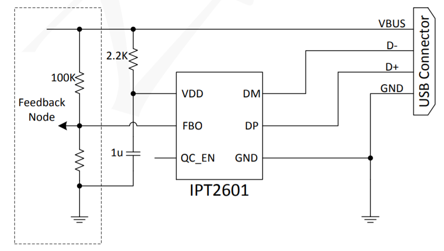
Fun fact: the datasheet is copyrighted by “FINE MAD ELECTRONICS GROUP”, as you can see in the datasheet’s footer.
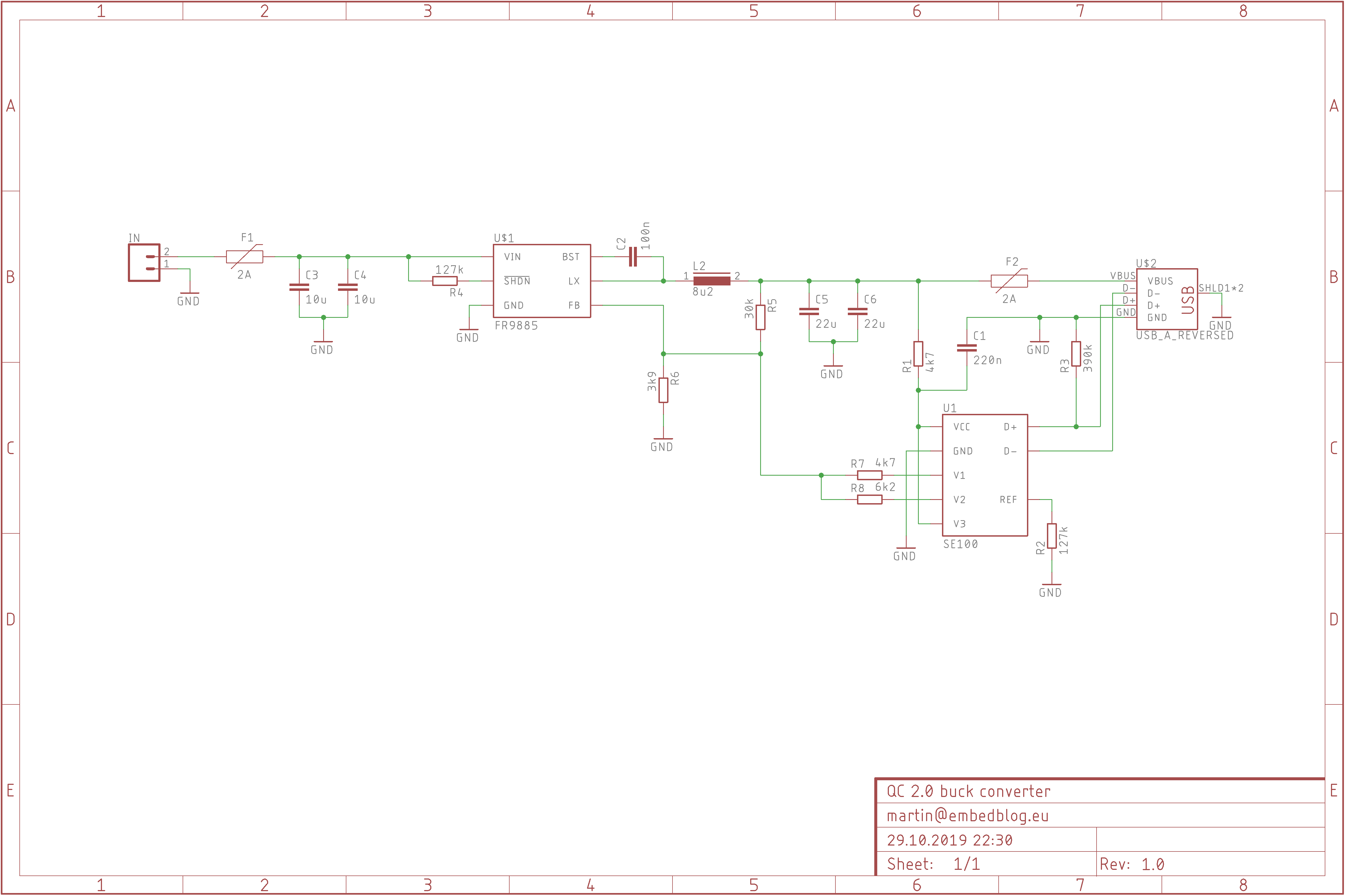
But back to the circuit – with so little information, I had to guess that it somehow injects (or sinks?) current from the feedback node. I assumed that the current flow is zero in 5 V output, and that the current is somewhat adjusted for the 100 kΩ resistor. With this, I calculated the bottom resistor of the divider. And heureka, it worked! So now I have a QC 3.0 compatible buck converter:
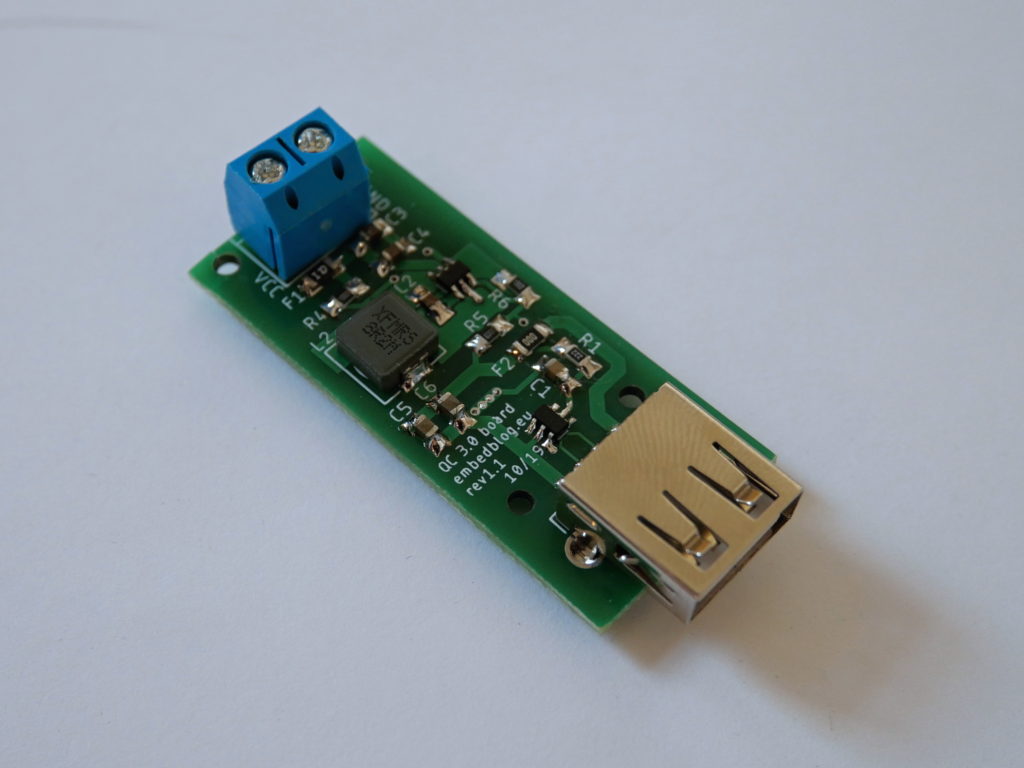
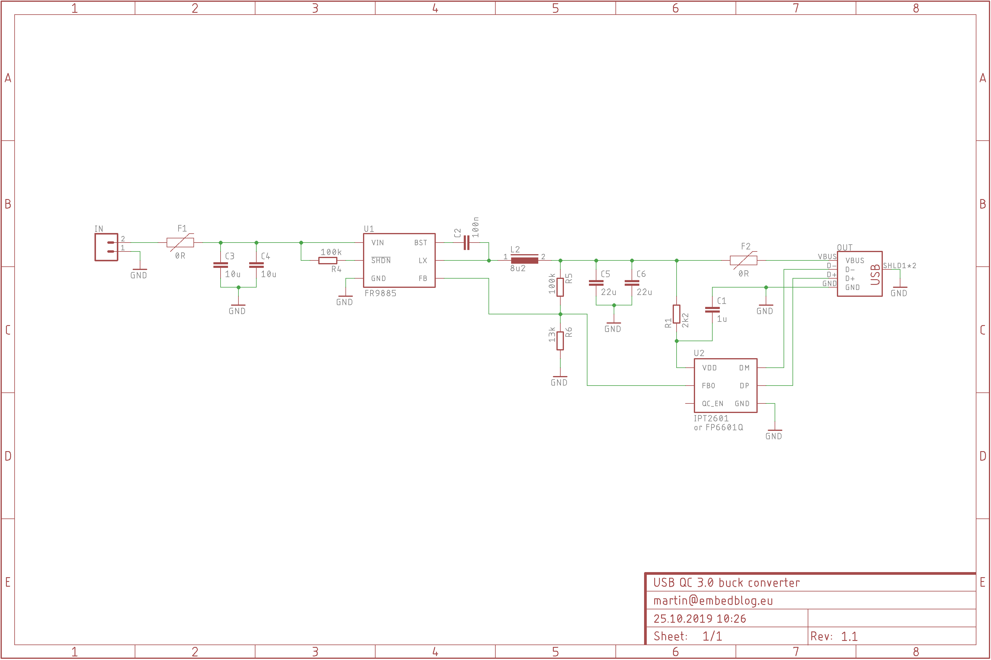
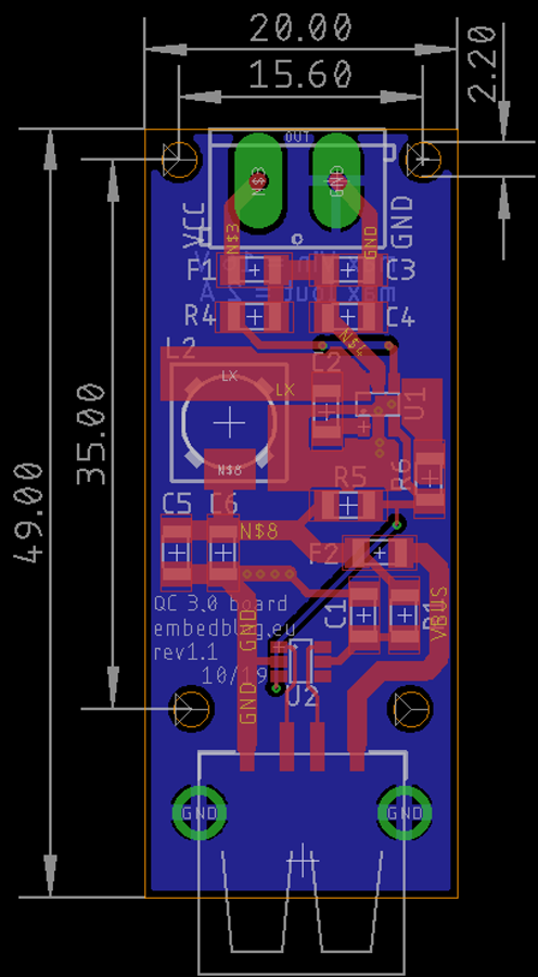
Both of the abovementioned boards utilize the FR9885, which is a buck controller IC with integrated high and low side mosfets. So you simply add one inductor, three resistors and five capacitors and you have a working switching regulator.
You could do the same with a boost converter IC and power it from a single 18650 Li-Ion cell, let’s say. But you’d need a really good switching converter, as boosting 3,7 V to 12 V at these currents isn’t trivial.
I later found out that the FP6601 is basically the same as the IPT2601, so can use either of them, there are no diferences that I am aware of.
Update 03/2020: Based on some more experiments, the FP6601 is actually better – for example, my Huawei phone won’t Quick Charge with the IPT2601, but with the FP6601, it quick charges at full 18 W.
Specs
- input voltage: 6 – 15 V, recommended 12 – 15 V
- input current: max 2 A
- output current: max 2 A
- efficiency (Vin = 12 V, Vout = 5 V, Iout = 1 A): 95 %
- efficiency (Vin = 12 V, Vout = 5 V, Iout = 2 A): 92 %
- quiescent current (no load connected, Vin = 12 V): 800 μA
Supported protocols
- HiSilicon Fast Charging Protocol (FCP), ie Huawei phones (tested)
- Qualcomm Quick Charge 2.0/3.0 Class A: up to 12 V Output Voltage (tested)
- USB DCP (shorting D+ Line to D-) per USB Battery Charging Specification, Revision 1.2 (tested)
- USB DCP (applying 2.7V on D+ Line and 2.7V on D- Line), ie Apple 12 W
- USB DCP (applying 1.2V on D+ and D- Lines)
- Chinese Telecommunication Industrial Standard YD/T 1591-2009 (whatever that is, I have not tested that)
The Charginator
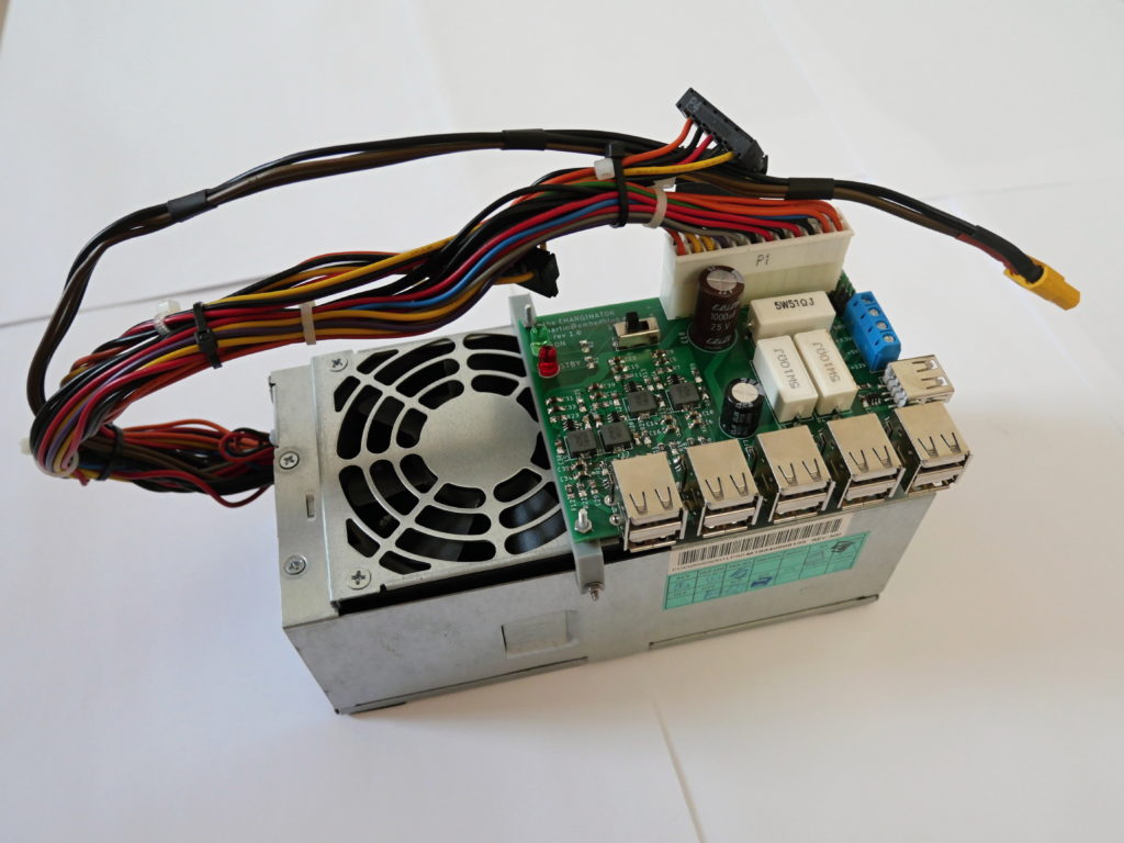
I also created a board for charging up to 11 devices from a single ATX power supply, see the Hackaday article here.
Conclusion
I was really happy that I managed to make this work, because as I already mentioned, there are almost no other schematics on how to do this on the internet. The result works fine, the buck driver IC does not heat up too much even at full load, so that’s cool (literally). The only thing I had slight problems with were the fuses – I wanted to use resetable PTC fuses, but these are really hard to come by for the currents and voltages I needed, so as of now, I am relying on the buck converters internal current limiting.
You can download the source in Eagle from my Github. Also, I put these handy boards for sale on Tindie.
Additional reading
- SE100 datasheet
- IPT2601 datasheet
- Adafruit MintyBoost – there is a nice discussion about different USB charging protocols
Notes
The only reason why I mentioned LCSC.com is because that’s where I found and got the chips from. But I am not endorsed, sponsored or whatever by them.
Update 04/2020: Minor corrections and tweaks. Added link to the Charginator.
Ahoj! Dont be afraid of smaller components packages – 0603 capacitors are as easy to solder as 1206 are. I can solder 0402 components with good light at my desk. Another thing worth mentioning is that ceramic capacitors capacitance depends from voltage, the greater the voltage the smaller the capacity. So small electrolythic capacitor at the input is required 35V/100u. Lx trace should be as thin as posible because of high frequency(trace thickness should support current). You can find many great examples of switching converters layouts at Richtek and Texas Instruments websites. Since
buck converters are simple I encourage You to make pcbs at home just to test the design. I wonder what you will use to power this converter? Your pcb design should look like the reference design from the pdf. Input capacitors should be put really close to input and ground shoulnd be splited!. BTW You can download some helpfull aps like LTspice and SATURN pcb toolkit. If you use STEAM send me an email with user name or code so I can add you. I dont use social media only STEAM.
Hi,
thanks for you advice. However, I have a reason to do things this way:
– I can solder 0402 as well, but I have a large stock of 1206 and 0805, so I am using these as of now; also, 0805 are faster to handle I’d say
– the input capacitors are per the datasheet of the switching regulator, so I guess the datasheet knows what it’s claiming?
– I am aware of the LX trace not being ideal, but I needed to dissipate heat from the IC
– I do not really see a reason to split ground in this case
Regards, M.
Could you add one additional USB charging port by just running additional wires to the same points for the USB port?
If I understand your question correctly, yes. In other words, if you have a lets say 12 V power supply, you can connect like 4 of these modules in parallel and have 4 USB ports.
Kinda sorta what I was saying. So lets say I have a 12v power supply. count the core of one module be used to supply two USB ports; or would you need to have a charge controller chip for each specific USB port?
You’d need one module per USB port.
Thanks so much for the guide!!
Have you tried the IPT2601Q (LCSC# C841224) and it’s ability to fast charge the Huawei at 18w? Seems the IPT2601 (LCSC# C190620) is being discontinued, but I can’t find details on what the difference is. There’s a datasheet I found listing the Q as 12v and F as 9v. Do you think the one you tested was the F variant?
Hi,
interesting. I do believe I was capable of getting 12 V out of it at some point, so this is a curious question – but one I cannot answer, unfortunately…
I ended up getting my board made and everything works fine. Thanks again for the post. These little QC controllers are great! Also got some all-in-one PD controller/buck converter chips for some USBC ports.
Did you ever run into any issues with the voltage going to the controller chip being too high? I’ve had no problems yet, but the datasheets says max voltage for VDD 6.5v. When QC is enabled, and at 12v, that would be too high. But It still seems to work. Datasheet example schematic also has the VDD tied directly to the VBUS with a 2.2k resistor…
Hi, glad it helped!
Regarding your question – I believe that there’s a zener inside the chip from VDD to ground – that’s why there’s the 2.2k resistor and the capacitor. I bet that if you supply 12 V to the circuit and then measure the VDD pin, there will be like 5 V or something similar… (I’ve seen this on some other IC’s before, this one doesn’t show the internal structure unfortunately).
You are correct! Reads a little less than 5v. Makes me feel better. Thanks for the reply!
Hi,
interesting project you did there.
I was wondering if I could apply it with a qc3.0 anker powerbank to power a lcd driver board with 12v at 2A?
The Postbank is capable of delivering up to 12v with 2.1A.
The driver board itself draws only 5v when connected to the USB from the powerbank.
So far my only alternative seems to be an arduino powered solution, which could do the chore of being the controller..
Hi,
I think you are mistaking the role of this device – this is a Quick Charge Source, not Sink, ie. something like that would be in the Anker Powerbank you mentioned…