Efficiency & noise of an MT3608 boost module
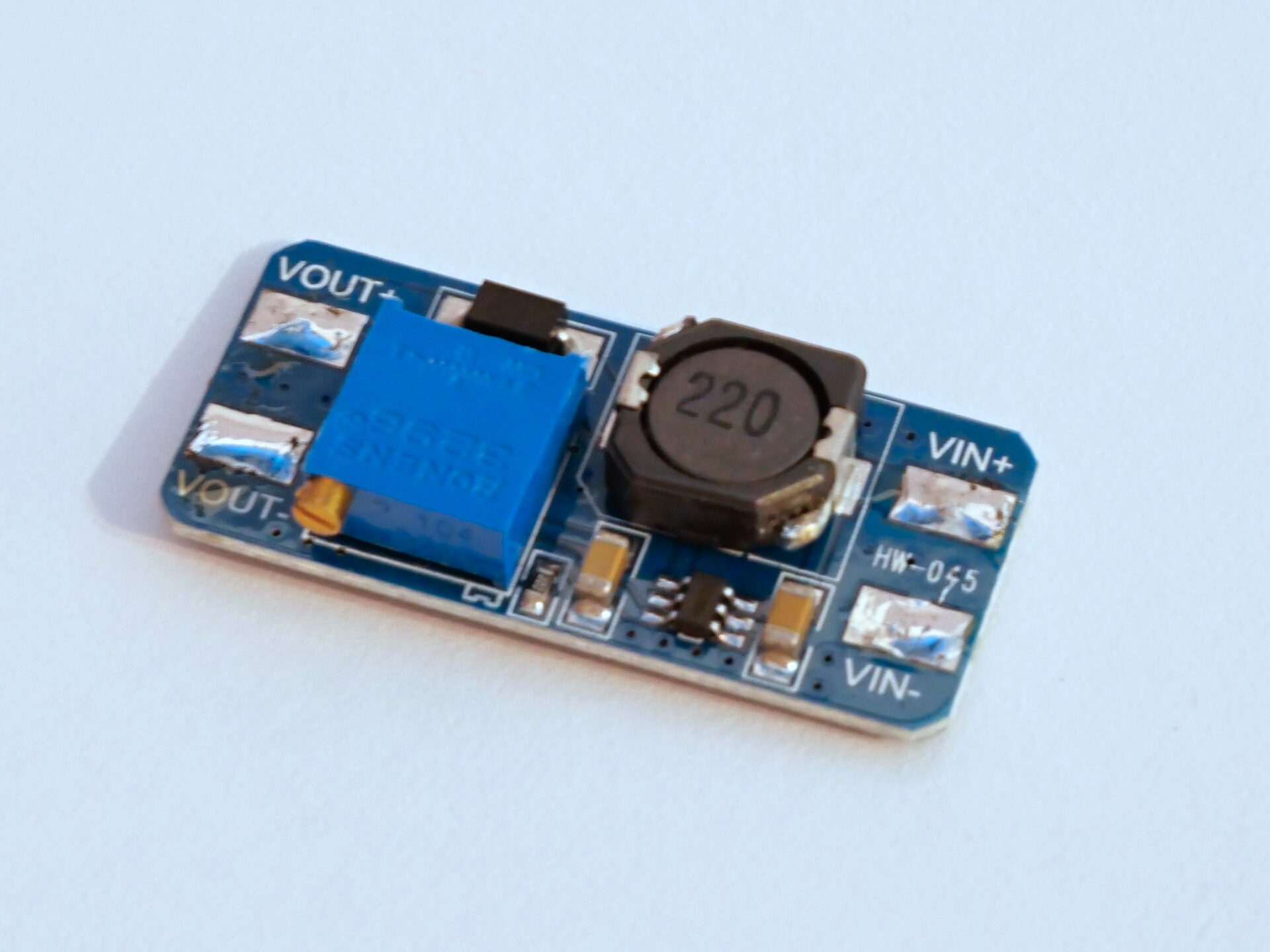
As part of theoretical research for a possible future project I wanted to measure the efficiency, noise and also max output current of an MT3608-based board, powered by a single 18650 battery. As my test subject I chose one of those cheap boards from Ebay, which you can get for about a dollar a piece.
Efficiency
The datasheet for the driving chip (MT3608) already has an efficiency chart for boosting to 12 V, but it’s from a 5 V supply and well, who believes Chinese datasheets? So I set the module’s output voltage to 12.4 V and used my electronic load to increase the load current until I hit a 2 A draw on the input. Voltages were measured directly at the module’s input and output terminals and a linear lab bench power supply was used instead of a battery, in order to supply the varying input voltages. And here are the results (notice that the efficiency axis starts at 70 %; also, click on the image for a larger version):
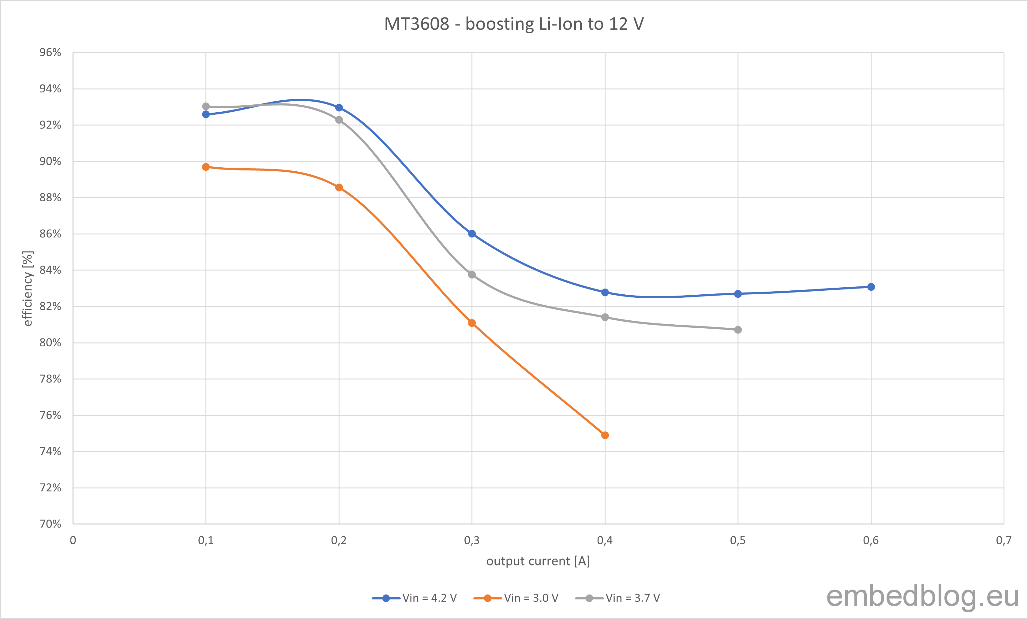
Practically speaking, the MT3608 is capable of boosting LiIon up to 12 V and 400 mA at all conditions. And at higher cell voltages you can draw up to 600 mA. Sure, you could push the module even more, but the IC and diode will start heating up a lot. Even during my tests it reached temperatures between 60 and 70 °C.
Output noise
I was also interested in the output noise – this is of course a switching regulator, so it will be noisy, but exactly how much?
As far as test setup goes, I used two channels in AC mode (with a 20 MHz BW limiter) of my oscilloscope as a pseudodifferential probe (setup recommended by Dave Jones in one his videos) directly on the output pads of the module. The output was also connected to a power resistor, drawing about 400 mA. Power was provided by a LiIon battery thru a classical DW01 protection circuit. Now this is the waveform I got:
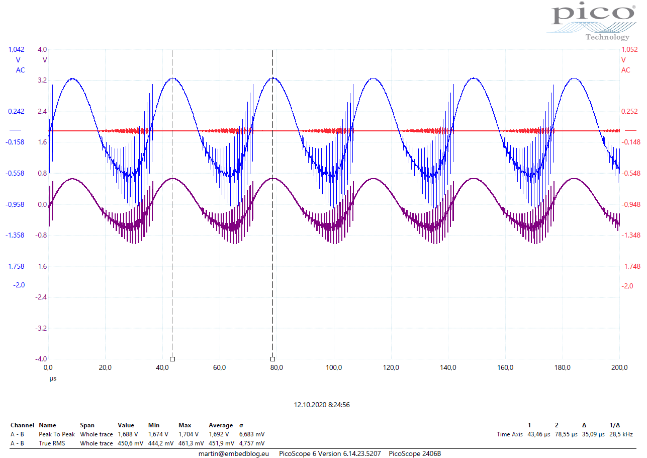
Here the purple waveform is the differential (math) channel. Numerically speaking, the RMS ripple was 450 mV and peak-to-peak ripple was 1.7 V!
Of course, boost converters are much more prone to noise, because the switching happens after the inductor – in a classical buck converter, on the contrary, the switching happens before the inductor, thus the inductor forms an LC filter on the output, greatly smoothing any ripple.
So that’s what I tried next – I added an LC filter on the output, consisting of a 8.2 µH inductor and a 220 µF electrolytic capacitor. Such an LC filter should have a cutoff frequency of 3.7 kHz, thus smoothing the large 30 kHz ripple on the output. Here is the result:
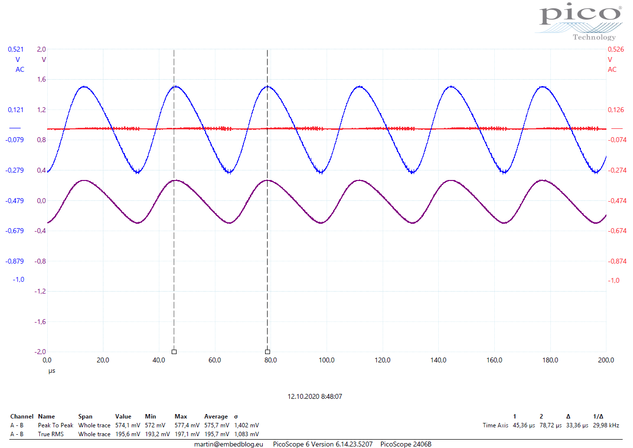
The filter greatly smoothed the HF ripple, superimposed on the LF sinewave. Even the sinewave got smoothed – notice that the vertical axis now has now half as much volts per division. So the resulting noise is now 200 mV RMS and 600 mV peak to peak. In other words, assuming we have just the 29 kHz sinewave, we achieved voltage gain of -9.35 dB, according to the clasical formula:
A_V = 20log_{10}(\frac{V_{OUT}}{V_{IN}})\quad[dB](Yeah, I really wanted to test out the KaTeX plugin for WordPress.)
In my project, I’ll probably use a 22 uH inductor to optimize BOM – the same value is used in the DC-DC regulator itself- so this bigger inductor should reduce noise even more.
Heat dissipation tip
This board contains two components which tend to heat up – the diode and and the IC itself. There isn’t much you can do about the diode, other than provide a large copper area with thermal vias around cathode (anode is switching at HF and it is recommended to keep the copper area as small as possible here).
The IC is in the SOT23-6 package, which isn’t really suitable for any sort of heat dissipation. But, if you look at the pinout below, you can see that right side of the IC contains pins IN, EN and NC. If you do not need the EN functionality (which is a little bit useless on a boost converter anyways, since it does not disconnect the load), you can connect all three of those pins together to the input.
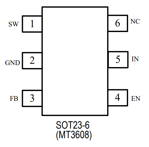
I also made a huge copper area with one large opening in the silkscreen for all three pins, hoping to make one large blob of solder, connecting all three pins together. This should again improve heat dissipation (but don’t expect miracles, it will still be limited by the bonding wires inside the IC itself).
I’ll update this with the actual picture once the PCB arrives.
Conclusion
I am currently building a simple, portable power supply – it’s nothing fancy, just an 18650 with charging and protection, digitally adjustable MT3608 boost circuit with an output filter and an OLED screen for displaying voltage and current. It will be part of a test setup for a certain commercial project.
Hey, I like the project you did here. But I am wondering, why did you use a differential probing method to measure the output noise. Why did you not use the AC-coupling on the oscilloscope, and measure the noise using one scope channel connected over the output of the converter?
Hi,
actually, I had the probes in AC mode. But what I learned the hard way when measuring output noise of my linear lab power supply is that the amount of noise superimposed on the resulting waveform with a single-ended measuremtn is just too much, so I had to use the differential method to get rid of the common mode noise. Sure, here it is probably an overkill, but I wanted to be on the safe side…